| Graphene production |
| The quality of graphene plays a crucial role as the presence of defects, impurities, grain boundaries, multiple domains, structural disorders, wrinkles in the graphene sheet can have an adverse effect on its electronic and optical properties. In electronic applications, the major bottleneck is the requirement of large size samples, which is possible only in the case of CVD process, but it is difficult to produce high quality and single crystalline graphene thin films possessing very high electrical and thermal conductivities along with excellent optical transparency. |
| Another issue of concern in the synthesis of graphene by conventional methods involves the use of toxic chemicals and these methods usually result in the generation hazardous waste and poisonous gases. Therefore, there is a need to develop green methods to produce graphene by following environmentally friendly approaches. The preparation methods for graphene should also allow for in-situ fabrication and integration of graphene-based devices with complex architecture that would enable eliminating the multi step and laborious fabrication methods at a lower production cost (read more: "Mass production of high quality graphene: An analysis of worldwide patents"). |
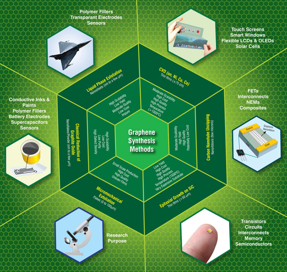
| Currently, the most common techniques available for the production of graphene are shown schematically below, which includes micromechanical cleavage, chemical vapor deposition, epitaxial growth on SiC substrates, chemical reduction of exfoliated graphene oxide, liquid phase exfoliation of graphite and unzipping of carbon nanotubes. However, each of these methods can have its own advantages as well as limitations depending on its target application(s). In order to surmount these barriers in commercializing graphene, concerted efforts are being made by researchers at various R&D institutes, universities and companies from all over the globe to develop new methods for large scale production of low-cost and high quality graphene via simple and eco-friendly approaches. |
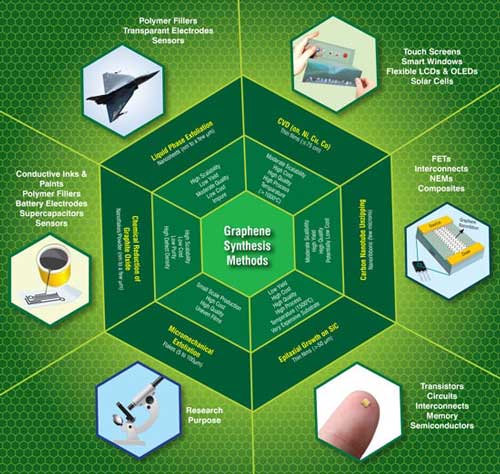 |
| A schematic showing the conventional methods commonly used for the synthesis of graphene along with their key features, and the current and future applications. (Image: CKMNT) (click image to enlarge) |
|
| Graphene-based nanomaterials have many promising applications in numerous areas: |
| Energy |
| Graphene-based nanomaterials have many promising applications in energy-related areas. Just some recent examples: Graphene improves both energy capacity and charge rate in rechargeable batteries; activated graphene makes superior supercapacitors for energy storage; graphene electrodes may lead to a promising approach for making solar cells that are inexpensive, lightweight and flexible; and multifunctional graphene mats are promising substrates for catalytic systems. |
| These examples highlight the four major energy-related areas where graphene will have an impact: solar cells, supercapacitors, lithium-ion batteries, and catalysis for fuel cells. An excellent review paper ("Chemical Approaches toward Graphene-Based Nanomaterials and their Applications in Energy-Related Areas") gives a brief overview of the recent research concerning chemical and thermal approaches toward the production of well-defined graphene-based nanomaterials and their applications in energy-related areas. The authors note, however, that before graphene-based nanomaterials and devices find widespread commercial use, two important problems have to be solved: one is the preparation of graphene-based nanomaterials with well-defined structures, and the other is the controllable fabrication of these materials into functional devices. |
|
| Sensors |
| Functionalized graphene holds exceptional promise for biological and chemical sensors. Already, researchers have shown that the distinctive 2D structure of graphene oxide (GO), combined with its superpermeability to water molecules, leads to sensing devices with an unprecedented speed ("Ultrafast graphene sensor monitors your breath while you speak"). |
| Scientists have now found that chemical vapors change the noise spectra of graphene transistors, allowing them to perform selective gas sensing for many vapors with a single device made of pristine graphene – no functionalization of the graphene surface required ("Selective gas sensing with pristine graphene"). |
| Quite a cool approach is to interface passive, wireless graphene nanosensors onto biomaterials via silk bioresorption as demonstrated by a graphene nanosensor tattoo on teeth monitors bacteria in your mouth. |
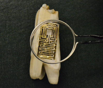 |
| Optical image of the graphene wireless sensor biotransferred onto the surface of a tooth. (Image: McAlpine Group, Princeton University) |
| Researchers also have begun to work with graphene foams – three-dimensional structures of interconnected graphene sheets with extremely high conductivity. These structures are very promising as gas sensors ("Graphene foam detects explosives, emissions better than today's gas sensors") and as biosensors to detect diseases (see for instance: "Nanotechnology biosensor to detect biomarkers for Parkinson's disease"). |
| Flexible, stretchable and foldable electronics |
| Graphene has a unique combination of properties that is ideal for next-generation electronics, including mechanical flexibility, high electrical conductivity, and chemical stability. Combine this with inkjet printing and you get an inexpensive and scalable path for exploiting these properties in real-world technologies ("Inkjet printing of graphene for flexible electronics"). |
| In contrast to flexible electronics, which rely on bendable substrates, truly foldable electronics require a foldable substrate with a very stable conductor that can withstand folding, i.e. an edge in the substrate at the point of the fold, which develops creases, and the deformation remains even after unfolding. That means that, in addition to a foldable substrate like paper, the conductor that is deposited on this substrate also needs to be foldable. To that end, researchers have demonstrated a fabrication process for foldable graphene circuits based on paper substrates. |
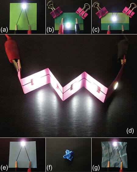 |
| Photographs of applications. a,b,c) Operation of a LED chip with graphene circuits on a paper substrate under -180° folding and 180° folding. d) Array of LED chips on a three-dimensional circuit board including negative and positive angle folding. e,f,g) Operation of a LED chip on the paper-based circuit board before and after crumpling. |
| Graphene's remarkable conductivity, strength and elasticity has made it a promising choice for stretchable electronics — a technology that aims to produce circuits on flexible plastic substrates for applications like bendable solar cells or robotic-like artificial skin. Scientists have devised a chemical vapor deposition (CVD) method for turning graphene sheets into porous three-dimensional foams with extremely high conductivity. By permeating this foam with a siloxane-based polymer, the researchers have produced a composite that can be twisted, stretched and bent without harming its electrical or mechanical properties ("Graphene: Foaming for stretchable electronics"). |
| Nanoelectronics |
| Some of the most promising applications of graphene are in electronics (as transistors and interconnects), detectors (as sensor elements) and thermal management (as lateral heat spreaders). The first graphene field-effect transistors (FETs) – with both bottom and top gates – have already been demonstrated. At the same time, for any transistor to be useful for analog communication or digital applications, the level of the electronic low-frequency noise has to be decreased to an acceptable level ("Graphene transistors can work without much noise"). |
| Transistors on the basis of graphene are considered to be potential successors for the some silicon components currently in use. Due to the fact that an electron can move faster through graphene than through silicon, the material shows potential to enable terahertz computing. |
| In the ultimate nanoscale transistor – dubbed a ballistic transistor – the electrons avoid collisions, i.e. there is a virtually unimpeded flow of current. Ballistic conduction would enable incredibly fast switching devices. Graphene has the potential to enable ballistic transistors at room temperature. |
| While graphene has the potential to revolutionize electronics and replace the currently used silicon materials ("High-performance graphene transistor with high room-temperature mobility"), it does have an Achilles heel: pristine graphene is semi-metallic and lacks the necessary band gap to serve as a transistor. Therefore it is necessary to engineer band gaps in graphene. |
| Experiments have demonstrated the benefits of graphene as a platform for flash memory which show the potential to exceed the performance of current flash memory technology by utilizing the intrinsic properties of graphene. |
| Photodetectors |
| Researchers have demonstrated that graphene can be used for telecommunications applications and that its weak and universal optical response might be turned into advantages for ultrafast photonics applications. They also found that graphene could be potentially exploited as a saturable absorber with wide optical response ranging from ultra-violet, visible, infrared to terahertz ("The rise of graphene in ultra-fast photonics"). |
| There is a very strong research interest in using graphene for applications in optoelectronics. Graphene-based photodetectors have been realized before and graphene's suitability for high bandwidth photodetection has been demonstrated in a 10 GBit/s optical data link ("Graphene photodetectors for high-speed optical communications"). |
| One novel approach is based on the integration of graphene into an optical microcavity. The increased electric field amplitude inside the cavity causes more energy to be absorbed, leading to a significant increase of the photoresponse ("Microcavity vastly enhances photoresponse of graphene photodetectors"). |
| Coatings |
| Coating objects with graphene can serve different purposed. For instance, researchers have now shown that it is possible to use graphene sheets to create a superhydrophobic coating material that shows stable superhydrophobicity under both static as well as dynamic (droplet impact) conditions, thereby forming extremely water repelling structures. |
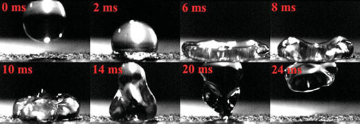 |
| Snapshots of a water droplet impacting the surface of the Teflon coated graphene foam. The impact velocity just prior to the droplet striking the surface was ∼76 cm/sec. The sequence of snapshots shows the deformation time history of the droplet upon impact. The droplet spreads, then retracts and successfully rebounds off the surface. The coefficient of restitution (i.e. ratio of droplet impacting velocity to ejecting velocity) is ∼0.37 for the Teflon coated foam. |
| Research findings also have established graphene as the world's thinnest known coating for protecting metals against corrosion. It was found that graphene, whether made directly on copper or nickel or transferred onto another metal, provides protection against corrosion. |
| Another novel coating application is the the fabrication of polymeric AFM probes covered by monolayer graphene to improving AFM probe performance. |
| Other uses |
| Researchers have exploited the extraordinary electrical and mechanical properties of graphene to create a very efficient electrical/sound transducer. This experimental graphene loudspeaker, without any optimized acoustic design, is simple to make and already performs comparably to or better than similar sized commercial counterparts, and with much lower power consumption. |
| Recent research also points to an opportunity to replacing antibiotics with graphene-based photothermal agents to trap and kill bacteria. |
| Graphene appears to be a most effective material for electromagnetic interference (EMI) shielding. Experiments suggests the feasibility of manufacturing an ultrathin, transparent, weightless, and flexible EMI shield by a single or a few atomic layers of graphene. |
| Due to rapidly increasing power densities in electronics, managing the resulting heat has become one of the most critical issues in computer and semiconductor design. As a matter of fact, heat dissipation has become a fundamental problem of electronic transport at the nanoscale. This is where graphene comes in – it conducts heat better than any other known material ("'Cool' graphene might be ideal for thermal management in nanoelectronics"). Thermal interface materials (TIMs) are essential ingredients of thermal management and researchers have achieved a record enhancement of the thermal conductivity of TIMs by addition of an optimized mixture of graphene and multilayer graphene ("Graphene sets new record as the most efficient filler for thermal interface materials"). |
| The concept of plasmonic cloaking is based on the use of a thin metamaterial cover to suppress the scattering from a passive object. Research shows that even a single layer of atoms, with the exciting conductivity properties of graphene, may achieve this functionality in planar and cylindrical geometries. This makes a single layer of graphene the thinnest possible invisibility cloak. |
| Over the last decade, various solid lubricant materials, micro/nano patterns, and surface treatment processes have been developed for efficient operation and extended lifetime in MEMS/NEMS applications, and for various fabrication processes such as nanoimprint lithography and transfer printing. One of the important considerations in applying a solid lubricant at the micro- and nanoscale is the thickness of the lubricant and the compatibility of the lubricant deposition process with the target product. Graphene, with its atomically thin and strong structural with low surface energy, is a good candidate for these applications ("Graphene - the thinnest solid lubricant"). |
| In the decades-old quest to build artificial muscles, many materials have been investigated with regard to their suitability for actuator application (actuation is the ability of a material to reversibly change dimensions under the influence of various stimuli). Besides artificial muscles, potential applications include microelectro-mechanical systems (MEMS), biomimetic micro-and nanorobots, and micro fluidic devices. In experiments, scientists have shown that graphene nanoribbons can provide actuation. |
| A relatively new method of purifying brackish water is capacitive deionization (CDI) technology. The advantages of CDI are that it has no secondary pollution, is cost-effective and energy efficient. Researchers have developed a CDI application that uses graphene-like nanoflakes as electrodes for capacitive deionization. They found that the graphene electrodes resulted in a better CDI performance than the conventionally used activated carbon materials ("Water desalination with graphene"). |
| Researchers demonstrated the use of graphene as a transparent conductive coating for photonic devices and show that its high transparency and low resistivity make this two-dimensional crystal ideally suitable for electrodes in liquid crystal devices (LCDs). |

No comments:
Post a Comment