Showing posts with label nanophotonics. Show all posts

Monday, 22 February 2016

Researchers at RMIT University and the University of Adelaide have joined forces to create a stretchable nano-scale device to manipulate light.

The device manipulates light to such an extent that it can filter specific colours while still being transparent and could be used in the future to make smart contact lenses.
                                                             
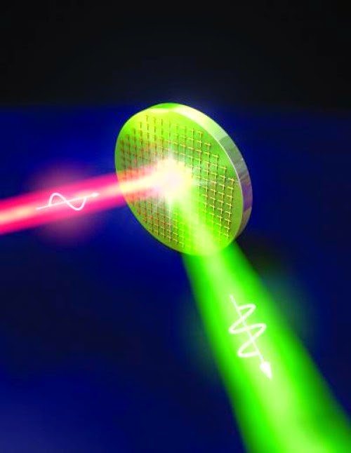
 nanoscale glass structures that filter or manipulate light
credit: RMIT/
The University of Adelaide
Using the technology, high-tech lenses could one day filter harmful optical radiation without interfering with vision – or in a more advanced version, transmit data and gather live vital information or even show information like a head-up display.

The light manipulation relies on creating tiny artificial crystals termed  “dielectric resonators”, which are a fraction of the wavelength of light – 100-200 nanometers, or over 500 times thinner than a human hair.

The research combined the University of Adelaide researchers’ expertise in interaction of light with artificial materials with the materials science and nanofabrication expertise at RMIT University.

Dr Withawat Withayachumnankul, from the University of Adelaide’s School of Electrical and Electronic Engineering, said: “Manipulation of light using these artificial crystals uses precise engineering.

“With advanced techniques to control the properties of surfaces, we can dynamically control their filter properties, which allow us to potentially create devices for high data-rate optical communication or smart contact lenses.

“The current challenge is that dielectric resonators only work for specific colours, but with our flexible surface we can adjust the operation range simply by stretching it.”

Associate Professor Madhu Bhaskaran, Co-Leader of the Functional Materials and Microsystems Research Group at RMIT, said the devices were made on a rubber-like material used for contact lenses.

“We embed precisely-controlled crystals of titanium oxide, a material that is usually found in sunscreen, in these soft and pliable materials,” she said.

“Both materials are proven to be bio-compatible, forming an ideal platform for wearable optical devices.

“By engineering the shape of these common materials, we can create a device that changes properties when stretched. This modifies the way the light interacts with and travels through the device, which holds promise of making smart contact lenses and stretchable colour changing surfaces.”

Lead author and RMIT researcher Dr. Philipp Gutruf said the major scientific hurdle overcome by the team was combining high temperature processed titanium dioxide with the rubber-like material, and achieving nanoscale features.

“With this technology, we now have the ability to develop light weight wearable optical components which also allow for the creation of futuristic devices such as smart contact lenses or flexible ultrathin smartphone cameras,” Gutruf said.

source ; RMIT news release link : click here

This post is copied from the materials in the RMIT website(news)

Monday, 28 July 2014

Building 'invisible' materials with light

 A new method of building materials using light, developed by researchers at the University of Cambridge, could one day enable technologies that are often considered the realm of science fiction, such as invisibility cloaks and cloaking devices.

    Although cloaked starships won't be a reality for quite some time, the technique which researchers have developed for constructing materials with building blocks a few billionths of a metre across can be used to control the way that light flies through them, and works on large chunks all at once. Details are published today (28 July) in the journal Nature Communications
                                                        
Building 'invisible' materials with light
          The key to any sort of 'invisibility' effect lies in the way light interacts with a material. When light hits a surface, it is either absorbed or reflected, which is what enables us to see objects. However, by engineering materials at the nanoscale, it is possible to produce 'metamaterials': materials which can control the way in which light interacts with them. Light reflected by a metamaterial is refracted in the 'wrong' way, potentially rendering objects invisible, or making them appear as something else.

         Metamaterials have a wide range of potential applications, including sensing and improving military stealth technology. However, before cloaking devices can become reality on a larger scale, researchers must determine how to make the right materials at the nanoscale, and using light is now shown to be an enormous help in such nano-construction.
The technique developed by the Cambridge team involves using unfocused laser light as billions of needles, stitching gold nanoparticles together into long strings, directly in water for the first time. These strings can then be stacked into layers one on top of the other, similar to Lego bricks. The method makes it possible to produce materials in much higher quantities than can be made through current techniques.

In order to make the strings, the researchers first used barrel-shaped molecules called cucurbiturils (CBs). The CBs act like miniature spacers, enabling a very high degree of control over the spacing between the nanoparticles, locking them in place.
In order to connect them electrically, the researchers needed to build a bridge between the nanoparticles. Conventional welding techniques would not be effective, as they cause the particles to melt. "It's about finding a way to control that bridge between the nanoparticles," said Dr Ventsislav Valev of the University's Cavendish Laboratory, one of the authors of the paper. "Joining a few nanoparticles together is fine, but scaling that up is challenging."
The key to controlling the bridges lies in the cucurbiturils: the precise spacing between the nanoparticles allows much more control over the process. When the laser is focused on the strings of particles in their CB scaffolds, it produces plasmons: ripples of electrons at the surfaces of conducting metals. These skipping electrons concentrate the light energy on atoms at the surface and join them to form bridges between the nanoparticles. Using ultrafast lasers results in billions of these bridges forming in rapid succession, threading the nanoparticles into long strings, which can be monitored in real time.

"We have controlled the dimensions in a way that hasn't been possible before," said Dr Valev, who worked with researchers from the Department of Chemistry and the Department of Materials Science & Metallurgy on the project. "This level of control opens up a wide range of potential practical applications."


source: University of Cambridge.Creative Commons Licence.

Tuesday, 8 July 2014

A simple and inexpensive fabrication procedure boosts the light-capturing capabilities of tiny holes carved into silicon wafers

Increasing the cost-effectiveness of photovoltaic devices is critical to making these renewable energy sources competitive with traditional fossil fuels. One possibility is to use hybrid solar cells that combine silicon nanowires with low-cost, photoresponsive polymers. The high surface area and confined nature of nanowires allows them to trap significant amounts of light for solar cell operations. Unfortunately, these thin, needle-like structures are very fragile and tend to stick together when the wires become too long.   

A straightforward procedure that transforms silver nanospheres (top) into silicon nanoholes (bottom) can overcome the shortcomings of nanowire-based solar cells

Now, findings by Xincai Wang from the A*STAR Singapore Institute of Manufacturing Technology and co-workers from Nanyang Technological University could turn the tables on silicon nanowires by improving the manufacturing of silicon ‘nanoholes’ — narrow cavities carved into silicon wafers that have enhanced mechanical and light-harvesting capabilities1.
Nanoholes are particularly effective at capturing light because photons can ricochet many times inside these openings until absorption occurs. Yet a practical understanding of how to fabricate these tiny structures is still lacking. One significant problem, notes Wang, is control of the initial stages of nanohole formation — a crucial period that can often induce defects into the solar cell.
Instead of traditional time-consuming lithography, the researchers identified a rapid, ‘maskless’ approach to producing nanoholes using silver nanoparticles. First, they deposited a nanometer-thin layer of silver onto a silicon wafer which they toughened by annealing it using a rapid-burst ultraviolet laser. Careful optimization of this procedure yielded regular arrays of silver nanospheres on top of the silicon surface, with sphere size and distribution controlled by the laser annealing conditions.
Next, the nanosphere–silicon complex was immersed into a solution of hydrogen peroxide and hydrofluoric acid — a mixture that eats away at silicon atoms directly underneath the catalytic silver nanospheres. Subsequent removal of the silver particles with acid produced the final, nanohole-infused silicon surface (see image).
The team analyzed the solar cell activity of their nanohole interfaces by coating them with a semiconducting polymer and metal electrodes. Their experiments revealed a remarkable dependence on nanohole depth: cavities deeper than one micrometer showed sharp drops in power conversion efficiency from a maximum of 8.3 per cent due to light scattering off of rougher surfaces and higher series resistance effects.
“Our simple process for making hybrid silicon nanohole devices can successfully reduce the fabrication costs which impede the solar cell industry,” says Wang. “In addition, this approach can be easily transferred to silicon thin films to develop thin-film silicon–polymer hybrid solar cells with even higher efficiency.”


source:  The Agency for Science, Technology and Research (A*STAR).

Thursday, 3 July 2014

Researchers invent 'meta mirror' to help advance nonlinear optical systems

Researchers at the Cockrell School of Engineering at The University of Texas at Austin have created a new nonlinear metasurface, or meta mirror, that could one day enable the miniaturization of laser systems.
                                                  
The invention, called a “nonlinear mirror” by the researchers, could help advance nonlinear laser systems that are used for chemical sensing, explosives detection, biomedical research and potentially many other applications. The researchers’ study will be published in the July 3 issue of Nature.
The metamaterials were created with nonlinear optical response a million times as strong as traditional nonlinear materials and demonstrated frequency conversion in films 100 times as thin as human hair using light intensity comparable with that of a laser pointer.
Nonlinear optical effects are widely used by engineers and scientists to generate new light frequencies, perform laser diagnostics and advance quantum computing. Due to the small extent of optical nonlinearity in naturally occurring materials, high light intensities and long propagation distances in nonlinear crystals are typically required to produce detectable nonlinear optical effects.
The research team led by UT Austin’s Department of Electrical and Computer Engineering professors Mikhail Belkin and Andrea Alu, in collaboration with colleagues from the Technical University of Munich, has created thin-film nonlinear metamaterials with optical response many orders of magnitude larger than that of traditional nonlinear materials. The scientists demonstrated this functionality by realizing a 400-nanometer-thick nonlinear mirror that reflects radiation at twice the input light frequency. For the given input intensity and structure thickness, the new nonlinear metamaterial produces approximately 1 million times larger frequency-doubled output, compared with similar structures based on conventional materials.
“This work opens a new paradigm in nonlinear optics by exploiting the unique combination of exotic wave interaction in metamaterials and of quantum engineering in semiconductors,” said Professor Andrea Alu.
The metamaterial at the basis of this unusual optical response consists of a sequence of thin layers made of indium, gallium and arsenic on the one hand and aluminum, indium and arsenic on the other. The researchers stacked approximately 100 of these layers, each between 1 nanometer and 12 nanometers thick, and sandwiched them between a layer of gold at the bottom and a pattern of asymmetric gold nanocrosses on top. The thin semiconductor layers confine electrons into desired quantum states, and gold nanocrosses resonate at input and output frequencies to enable the the nonlinear optical response of the mirror.
The realized mirror converts light from a wavelength of 8 micrometers to 4 micrometers; however, the structures can be tailored to work at other wavelengths, from near-infrared to mid-infrared to terahertz.
“Alongside frequency doubling, our structures may be designed for sum- or difference-frequency generation, as well as a variety of four-wave mixing processes,” said UT Austin graduate student Jongwon Lee, the lead author on the paper.
“Our work unveils a pathway towards the development of ultrathin, highly nonlinear optical elements for efficient frequency conversion that will operate without stringent phase-matching constraints of bulk nonlinear crystals,” said Professor Mikhail Belkin.
Belkin and Alu led a team of researchers that included electrical and computer engineering graduate students Jongwon Lee, Mykhailo Tymchenko and Feng Lu. Pai-Yen Chen and Christos Argyropoulos, who graduated from the Cockrell School in 2013, also contributed to the paper. The semiconductor material was grown at the Walter Schottky Institute, Technical University of Munich.
The research was funded by the National Science Foundation, the Air Force Office of Scientific Research and the Office of Naval Research, as well as the German Research Foundation.
The University of Texas at Austin is committed to transparency and disclosure of all potential conflicts of interest. All UT investigators involved with this research have filed their required financial disclosure forms with the university. Alu and Belkin have both received research funding for other projects from the National Science Foundation and other major public science foundations. Belkin has also received research funding for other projects from the companies Omega Optics, Anasys Instruments and Hamamatsu Photonics, and Alu from the AEgis Technologies Group. An alumnus and former doctoral student who worked on the project, Pai-Yen Chen, now works for Intellectual Ventures Inc

source : The University of Texas at Austin